只需一步,快速开始
微信扫一扫,快速登录
您需要 登录 才可以下载或查看,没有账号?立即注册
使用道具 举报
6月12日优惠券商品合集-越南火鸡
6.12 京东+淘宝618红包!合金筷1
6月12日优惠券商品合集-颈椎腰椎
6.12 京东+淘宝618红包!粽子140
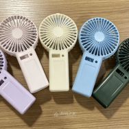
21700双锂电池暴力风扇 2204穿越
6月12日优惠券商品合集-红枣2斤6
本版积分规则 发表回复 回帖并转播 回帖后跳转到最后一页
APP|手机版|小黑屋|关于我们|联系我们|法律条款|数码之家-技术知识分享平台
闽公网安备35020502000485号
闽ICP备2021002735号-2
GMT+8, 2026-6-12 13:11 , Processed in 0.280800 second(s), 11 queries , Gzip On, Redis On.
Powered by Discuz!
© MyDigit.Net Since 2006


 IP归属地
IP归属地 雷达卡
雷达卡 发表于 2019-3-28 18:58:38


 提帖卡
提帖卡 置顶卡
置顶卡 锁帖卡
锁帖卡 解锁卡
解锁卡 显目卡
显目卡 千斤顶
千斤顶 楼主
楼主 发表于 2019-3-28 22:31:44